News ·
Royma RMCT2000 resolves sub-micron detail for MEMS micro CT inspection
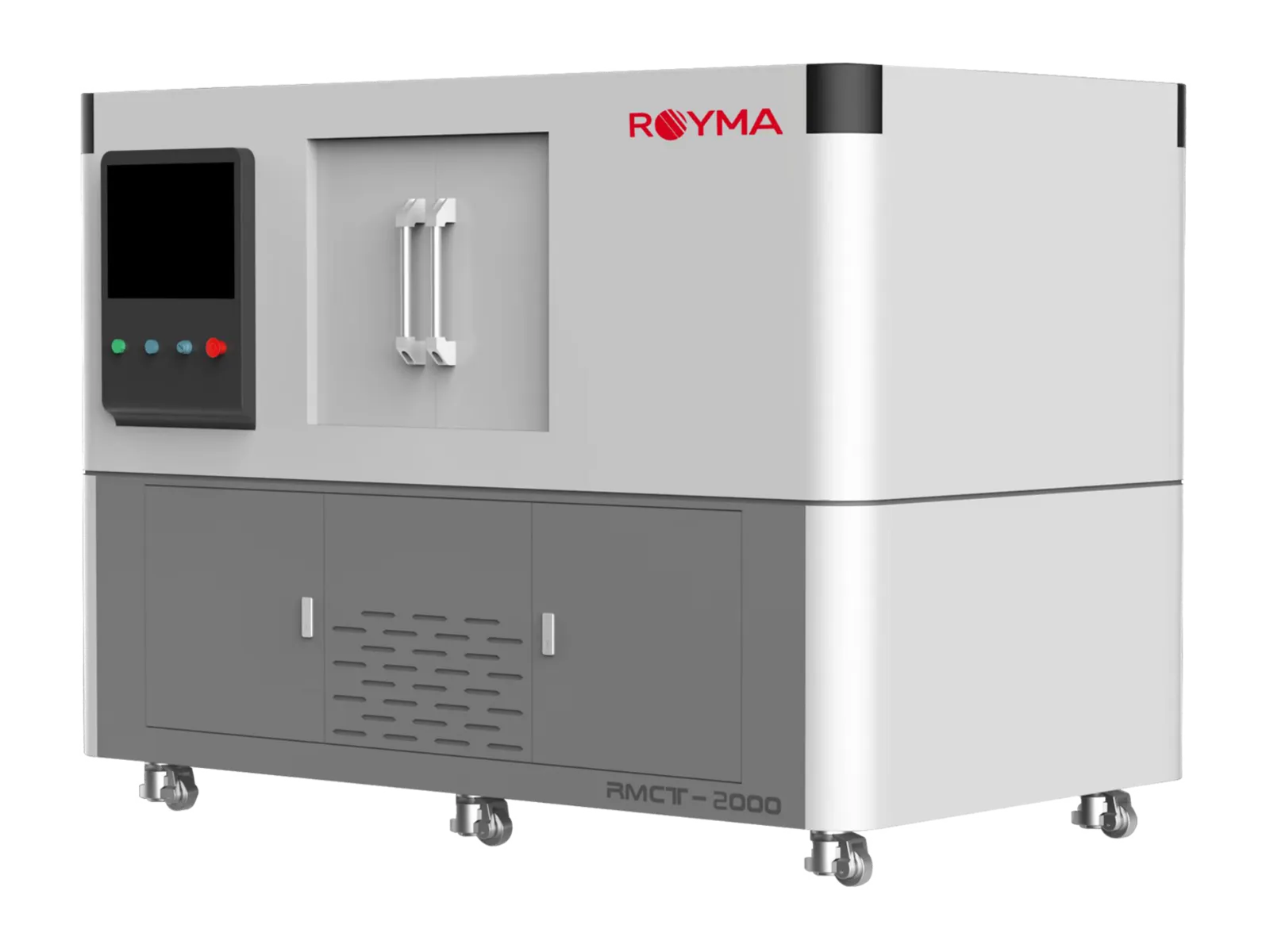
Royma brings sub-micron MEMS micro CT inspection to the failure-analysis lab with the RMCT2000, a laboratory CT system with a 190 kV open nanofocus X-ray source and a stated JIMA resolution of 0.5 µm. The RMCT2000 scans MEMS devices and heterogeneously integrated packages in 3D and shows cavities, bonds and buried interfaces without cross-sectioning the part.
The RMCT2000 combines two switchable source and detector configurations in one cabinet. In nanofocus mode, the open 190 kV source works with a detector of 49.5 µm pixel pitch and a 4608 × 5890 pixel matrix. In microfocus mode, a 225 kV, 350 W source with a stated JIMA resolution of 2 µm and a 3072 × 3072 pixel detector takes larger and denser assemblies. The engineer chooses the mode by the size of the part and the smallest feature to be resolved.
- Nanofocus mode: 190 kV open source, JIMA 0.5 µm, samples up to 5 kg
- Microfocus mode: 225 kV and 350 W, JIMA 2 µm, parts up to 15 kg
- Measurement: stated accuracy of 3.0 + L/50 µm
- Scan modes: circular, helical, segmented and stitch scanning, jitter-artefact removal
- Mechanics: five control axes, n × 360° rotation
Sub-micron detail inside the closed device
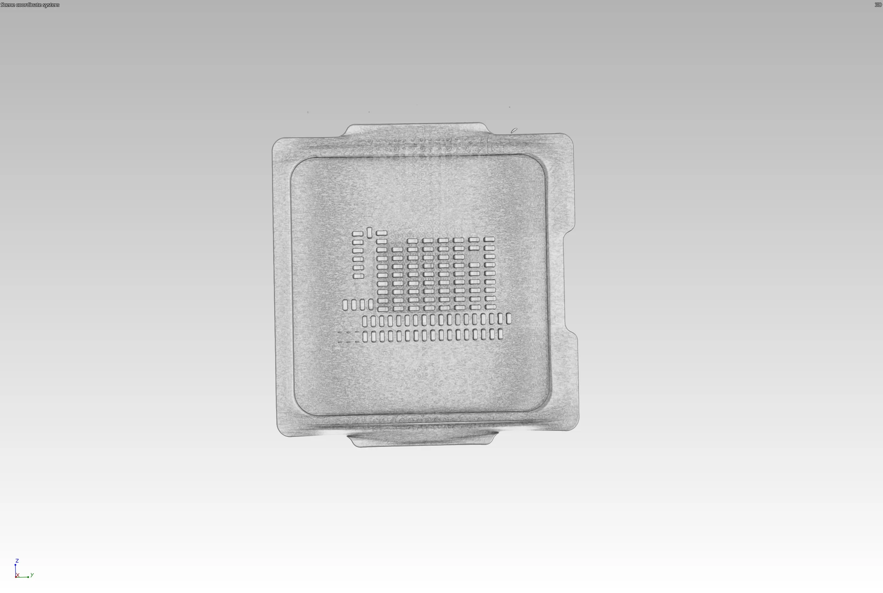
A MEMS device keeps its function behind a cap, a lid or a bonded wafer stack. The RMCT2000 looks through that closure and shows what lies beneath it: the shape of the cavity, the continuity of the bond frame, the position of the moving structure and any particle trapped inside. Because the scan is non-destructive, the same device stays available for electrical test, reliability stress or a later physical analysis at the exact location the CT data points to.
The nanofocus source resolves features at sub-micron scale on small samples. That suits bond wires, micro-bumps, through-silicon vias and the thin interfaces between stacked dies. Micro-voids, micro-cracks, inclusions and delamination at these interfaces appear in the reconstructed volume as slices in any orientation, without the preparation artefacts of grinding or polishing.
“The RMCT2000 shows a failure-analysis engineer the inside of a closed MEMS device or a chip stack before anyone cuts it,” says Gabor Szabo, Sales Director Europe, Royma Europe. “The engineer then sections only where the CT volume shows a defect.”
One cabinet for the device and the package
Heterogeneously integrated devices combine dies, interposers, substrates and moulding compound of very different density in one package. The RMCT2000 covers both ends of that range in a single system. Nanofocus mode resolves the finest structures of the die stack and its interconnects; microfocus mode, at 225 kV and 350 W, penetrates the complete package, the board-level assembly or a tray of parts up to 15 kg.
Helical, segmented and stitch scanning extend the scanned volume beyond a single standard scan when a sample is taller or wider than one detector image. Jitter scanning with artefact removal keeps thin interfaces and small voids readable in the reconstruction. The five-axis manipulator positions the region of interest for each scan.
Measurement as well as imaging
The RMCT2000 states a measurement accuracy of 3.0 + L/50 µm, so the same scan that shows a defect also returns dimensions. Engineers can measure bond-line thickness, cavity height, bump height and die tilt from the volume and compare them with the design.
Typical tasks for the RMCT2000 in MEMS and advanced packaging:
Inspection of MEMS sensors and actuators for cavity shape, bond-frame continuity and trapped particles; analysis of wire bonds, flip-chip bumps and through-silicon vias in stacked dies; detection of voids and delamination in die attach and underfill; and dimensional checks of package geometry against the design data. Royma also offers the RMCT2000 for mini-LED dies and consumer-electronics components, where the same sub-micron detail applies.
“With one RMCT2000, a lab moves from the single die to the finished package without changing system,” adds Szabo. “We scan customer samples in both modes and show which configuration gives the clearest result for their device.”
More on the system on the RMCT2000 machine page and on CT for semiconductors and consumer electronics.
Test scans available
Royma Europe offers test scans of customer MEMS devices and packages on the RMCT2000. Contact Adrian de Riz, Sales Director, Royma Europe, adrian_deriz@roymatek.eu, +49 511 57092696 – www.roymatek.jp.
Royma Europe, Leibniz Universität Hannover – Institut für Produktentwicklung und Gerätebau, Gebäude 8143, An d. Universität 1, 30823 Garbsen, Germany.
About Royma: Royma Industrial CT develops and builds industrial X-ray and computed tomography systems, from 2D X-ray to horizontal, gantry, planar and inline CT, for battery, aerospace, semiconductor, casting, electronics and automotive manufacturing.